SEM Analysis Services
SEM Testing & Failure Investigations
Microstructural Analysis
Precision SEM testing for failure analysis, contamination studies, crystallography, and material validation using a Zeiss Scanning Electron Microscope.
When material behaviour matters, assumptions fail.
Microlab delivers clear, defensible SEM results you can act on.
- Zeiss Scanning Electron Microscope
- NABL ISO/IEC 17025 Accredited
- EDX • EDS • EBSD Analysis
NABL ISO/IEC 17025
Accredited
Zeiss SEM
Equipment
Expert Analysts
Not Just Operators
Fast Turnaround
Days, Not Weeks
SEM Analysis Services
When the Problem Is Microscopic, the Answer Has to Be Precise
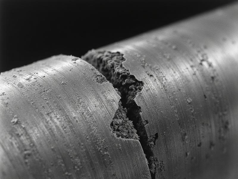
- Cracks that appear without warning.
- Coatings that peel too early.
- Components that fail despite meeting specifications.
These problems do not show up under optical microscopes.
SEM testing reveals what actually happened at the micro and nanoscale. At Microlab, we use a Zeiss Scanning Electron Microscope combined with EDX, EDS, and EBSD analysis to uncover surface morphology, elemental composition, crystallography, phase distribution, and stress-related indicators with clarity and confidence.
No overcomplication. No guesswork. Just answers.
Our Capabilities
What Our SEM Testing Delivers
Our SEM services are built around real industrial decisions, not academic demonstrations.
Scanning Electron Microscope (SEM)
High-resolution imaging for:
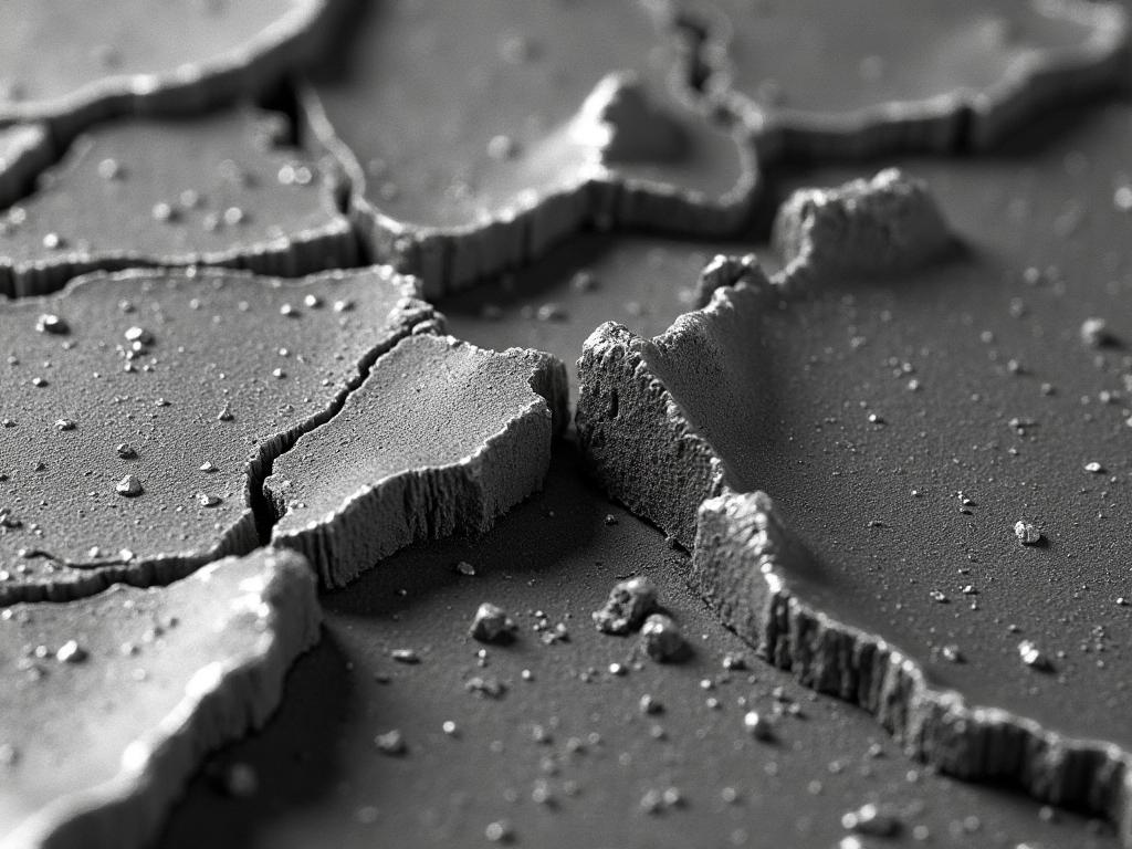
- Fracture surfaces and crack initiation
- Coating defects and delamination
- Wear, corrosion, and surface damage
- Microstructural features invisible to optical methods
EDX / EDS Analysis
Elemental composition analysis for:
- Contaminant and particle identification
- Alloy verification
- Inclusion and residue analysis
- Elemental mapping across critical regions
Combined SEM + EDX/EDS
Comprehensive analysis providing:
- Visual evidence with chemical confirmation
- Correlated morphology and composition data
- Defensible results for critical decisions
- Complete material characterization
Advanced Analysis
EBSD Testing, Crystallography & Phase Analysis
When structure defines performance, imaging alone is not enough.
EBSD Testing
- Grain size and grain orientation analysis
- Phase identification and phase distribution
- Crystallographic texture evaluation
- Metallurgical and process validation studies
Phase Analysis
- Multiphase alloys characterization
- Failure investigations linked to phase transformation
- Heat-treated components validation
- Critical metallurgical evaluation
Residual Stress Evaluation
- Stress concentration leading to cracking or distortion
- Failures with no obvious macroscopic cause
- Heat treatment or forming process investigation
- Stress-induced microstructural feature identification

Applications
Applications of Our SEM Testing
Clients approach Microlab when results must be technically sound and defensible.
Failure & Fracture Analysis
Root cause investigation for component failures
Contamination Identification
Particle and contaminant characterization
Coating Evaluation
Thickness and surface quality assessment
Phase Transformation
Studies of heat treatment effects
Crystallography & EBSD
Grain structure and orientation analysis
Residual Stress Investigation
Stress-related failure mechanisms
If the component failed unexpectedly, SEM explains why.
Materials We Analyze
Our SEM, EDX, EDS, and EBSD testing supports:
- Metals and alloys
- Coatings and thin films
- Polymers and plastics
- Powders, dust, and particulates
- Ceramics and composites
- Electronic and industrial components
If a sample is unsuitable, we say it upfront. No wasted time.
Industries Served
Industries That Rely on Our SEM Analysis
Microlab supports industries where precision is non-negotiable.
Manufacturing & Quality Control
Material verification, defect analysis, coating evaluation, and contamination studies.
Automotive & Auto Components
Failure analysis of engine parts, fasteners, welds, and wear-related issues.
Aerospace & Defense Suppliers
Crystallography, phase analysis, and microstructural validation for critical components.
Electronics & PCB Manufacturing
SEM and EDS analysis for solder joints, micro-cracks, and foreign particles.
Pharmaceuticals & Medical Devices
Surface morphology and contamination investigations using SEM-EDX.
Metallurgy & Metal Processing
EBSD testing, grain structure analysis, phase evaluation, and stress-related studies.
R&D and Research Laboratories
Advanced material characterization and process development support.
Different sectors. Same expectation: reliable SEM results.
Why Choose Us
Why Microlab Testing
This is where decisions are made.
- Zeiss Scanning Electron Microscope for stable, high-resolution imaging
- NABL ISO/IEC 17025 accredited quality systems
- Experienced SEM analysts, not just equipment operators
- Clear interpretation, not unreadable data dumps
- Reports structured for audits, CAPA, and engineering decisions
We don’t sell microscope hours.
We deliver clarity and accountability.

Our Process
Our SEM Testing Process
Simple. Controlled. Transparent.
Sample Review
Feasibility confirmation
Preparation
Controlled sample prep
SEM Imaging
Zeiss SEM analysis
Testing
EDX, EDS, or EBSD
Report
Findings & interpretation
No unnecessary steps. No delays caused by confusion.
FAQs
SEM, EDX, EDS & EBSD Testing
Common questions about our testing services
What is SEM testing used for?
SEM testing examines surface morphology, fractures, coatings, and microstructural features at very high magnifications.
Is there a difference between EDX and EDS analysis?
No. Both refer to Energy Dispersive X-ray Spectroscopy used for elemental analysis with SEM.
When is EBSD testing required?
Can SEM identify unknown contaminants or particles?
Yes. SEM combined with EDX or EDS is highly effective for unknown particle identification.
Do you perform phase analysis using SEM?
Yes. SEM with EBSD and EDS enables detailed phase analysis and phase distribution studies.
Is SEM testing destructive?
SEM is minimally destructive. Some samples may require surface coating, but the bulk material remains intact.
Can SEM detect residual stress?
SEM supports residual stress-related investigations by identifying stress-induced microstructural features and failure indicators.
What is the typical turnaround time?
Turnaround depends on sample type and scope. Standard SEM testing is usually completed within a few working days.
Do you provide interpretation or only images?
You receive interpretation. Images without conclusions are useless.
Request SEM Testing
If a material issue is delaying approval, production, or investigation, waiting only increases cost.
Speak with Microlab’s SEM experts today.
- ✓ NABL ISO/IEC 17025 Accredited
- ✓ Zeiss SEM Equipment
- ✓ Expert Interpretation Included